Tesla Terafab Silicon Strategy
On March 21, 2026, Elon Musk announced Terafab at the defunct Seaholm Power Plant in Austin, Texas — a joint venture between Tesla, SpaceX, and xAI to build what Musk described as "the most epic chip-building exercise in history by far." The announcement represents the most explicit Silicon Autonomy commitment ever made by a vehicle or robotics OEM, and the most ambitious vertical integration play in the semiconductor industry since TSMC was founded in 1987.
This page covers the deployment layer — what Terafab means for Tesla's vehicles, robots, energy infrastructure, and orbital compute ambitions. The chip architecture, fabrication process, and semiconductor supply chain upstream of Terafab are covered on SemiconductorX.
Why Tesla Is Building a Fab
The decision to build captive semiconductor manufacturing capacity is not a strategic preference — it is a supply chain forcing function. At Tesla's Q4 2025 earnings call, Musk explicitly warned that external foundry capacity from TSMC, Samsung, and Micron would hit a ceiling within three to four years given Tesla's combined demand across vehicles, Optimus robots, and AI training infrastructure.
The demand arithmetic is stark. Tesla's stated target of 100 million Optimus units annually would require north of 200 million chips per year for that product line alone, before accounting for the vehicle fleet, robotaxis, and AI inference workloads. No external foundry is sized or incentivized to prioritize a single customer's demand at that scale. Musk's framing was direct: "We either build the Terafab, or we don't have the chips, and we need the chips, so we build the Terafab."
A secondary forcing function is the D3 chip family — radiation-hardened processors for orbital compute. Radiation- and thermal-hardened processors for orbital compute represent a genuinely underserved niche that no major foundry prioritizes at volume. TSMC, Samsung, and GlobalFoundries serve commercial and hyperscaler demand — not the specific rad-hard, thermally hardened requirements of a satellite constellation running continuous AI inference in low Earth orbit. Tesla and SpaceX have a captive demand signal for D3 that no external foundry can or will address on their timeline.
Terafab: Structure and Scope
Terafab is a joint venture between Tesla, SpaceX, and xAI — consolidated under the SpaceX/xAI umbrella following the February 2026 SpaceX-xAI merger. The structural logic: SpaceX provides the orbital compute demand signal for D3 chips, xAI provides the AI model training and inference demand, and Tesla provides the vehicle and robotics inference demand for AI5. Together the three entities create a captive customer base that justifies the capital outlay no single entity could rationalize alone.
| Dimension | Detail |
|---|---|
| Announced | March 21, 2026 — Seaholm Power Plant event, Austin TX |
| Joint venture partners | Tesla, SpaceX, xAI (SpaceX subsidiary post-February 2026 merger) |
| Location | North Campus, GigaTexas, Austin TX — prototype fab. Full-scale location TBD |
| Estimated capital cost | $20–25 billion — not included in Tesla's 2026 capex guidance of $20B+ |
| Process node target | 2nm — most advanced node currently entering commercial production at TSMC |
| Compute output target | 1 terawatt of AI compute annually — approximately 70% of TSMC's current global output at full scale |
| Wafer starts target | 100,000 wafer starts per month (prototype); 1 million at full scale |
| Vertical integration scope | Chip design, lithography, fabrication, memory production, advanced packaging, testing — all under one roof |
| Output allocation | 80% orbital/space AI satellites, 20% ground-based (vehicles, robots, datacenters) |
| First product | AI5 chip — small batch 2026, volume production 2027 |
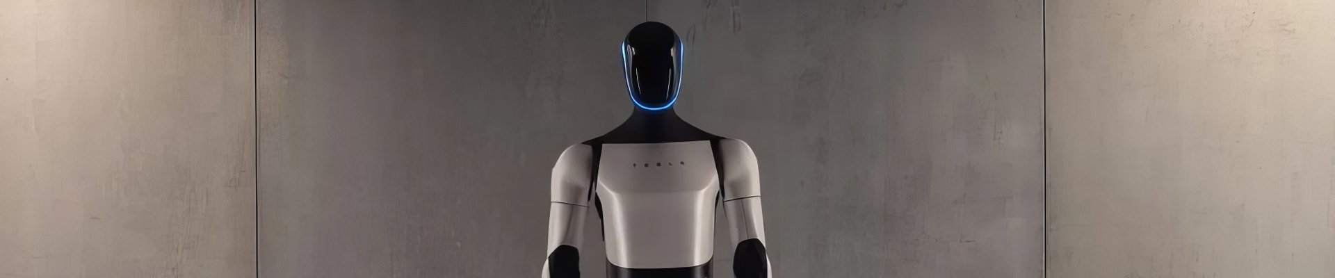
The AI5 Chip: Inference at the Edge
AI5 is Tesla's fifth-generation inference chip — the successor to the HW4 computer currently deployed in production vehicles. It is designed from first principles as a domain-specific inference accelerator: not a general-purpose GPU, but a chip optimized exclusively for Tesla's neural network workloads across vehicles, Optimus robots, and datacenter inference.
The architectural philosophy is deliberate narrowness. By eliminating components unnecessary for Tesla's specific use case — traditional GPU graphics subsystems, image signal processors, general-purpose compute blocks — Tesla has concentrated silicon area on the operations that matter: tensor multiplication, attention mechanisms, and the softmax function that governs neural network decision outputs. AI5 integrates the softmax algorithm natively — an operation that previously required 40 emulation steps on HW4 now runs in a single native operation.
| Specification | AI4 (Current) | AI5 (2026–2027) | Improvement |
|---|---|---|---|
| Inference performance | ~500 TOPS | ~5,000 TOPS | ~10x raw, 40x effective in FSD tasks |
| Raw compute | Baseline | 8x HW4 | 8x |
| Memory capacity | ~16GB | ~144GB | 9x |
| Memory bandwidth | Baseline | 5x HW4 | 5x |
| Power consumption (peak) | ~160W | 700–800W | 5x — higher absolute but 3x better efficiency per TOPS |
| Fabrication | Samsung 4nm | Samsung Taylor + TSMC Arizona (dual fab) | Dual-fab supply resilience |
| Softmax implementation | 40-step CPU emulation | Native single-step | 40x for this critical operation |
| Production timeline | Current production | Small batch 2026, volume 2027 | — |
The dual-fab strategy — splitting AI5 production between Samsung Taylor in Texas and TSMC in Arizona — provides supply resilience, competitive pricing pressure between fabs, and doubled production throughput. It also reflects Tesla's awareness that a single fab fire or export restriction cannot be allowed to halt vehicle and robot production.
AI5 Deployment Domains
AI5 is the first Tesla chip designed explicitly to serve three deployment domains from a single architecture — vehicles, robots, and datacenters. This convergence is the architectural expression of Tesla's vertical integration thesis: one chip family, optimized for Tesla's specific inference workloads, deployed everywhere Tesla operates.
| Domain | Platform | AI5 Role | Why AI5 vs External |
|---|---|---|---|
| Vehicles | Cybercab, Model 3/Y/S/X post-2027, future Tesla vehicles | FSD unsupervised inference — perception, prediction, planning at 15–30 Hz | Domain-specific architecture delivers 40x effective performance at fraction of NVIDIA cost per inference cycle |
| Humanoid Robots | Optimus — all generations post-AI5 availability | Locomotion control, manipulation planning, object recognition, continuous 15–30 Hz operation | Power efficiency critical in human-scale form factor — 3x efficiency improvement over AI4 extends operational runtime |
| Datacenter Inference | Cortex inference clusters — replacing Dojo for inference workloads | Fleet-scale inference processing — shadow mode data, edge case analysis, model evaluation | 10x lower inference cost vs NVIDIA H100 class hardware for Tesla-specific workloads |
The D3 Chip: Orbital Compute
D3 is the second Terafab chip family — and arguably the more strategically differentiated of the two. Where AI5 competes in a market served by NVIDIA, Qualcomm, and Mobileye, D3 addresses a market that essentially does not exist at production scale: radiation-hardened, thermally hardened AI inference processors for sustained operation in low Earth orbit.
Orbital compute imposes constraints that commercial silicon cannot meet:
Radiation hardening. Cosmic rays and solar particle events cause single-event upsets (SEUs) in standard CMOS logic — bit flips that corrupt computation. Radiation-hardened design uses triple-redundant logic cells, error-correcting memory, and specialized process options to maintain computational integrity through radiation events that would crash commercial silicon.
Thermal management in vacuum. Heat rejection in space cannot rely on convection — there is no atmosphere. All waste heat must be conducted to radiating surfaces. This constrains chip power density differently than terrestrial cooling — making Musk's claim that space solar irradiance at 5x Earth surface levels combined with vacuum heat rejection makes orbital compute thermally viable at scale a genuine engineering argument, not just a talking point.
Captive demand. SpaceX has applied to launch approximately one million data center satellites as part of a planned orbital AI constellation. That constellation requires chips that no foundry currently produces at volume. D3 is a vertical necessity — not a market opportunity.
| Dimension | AI5 (Terrestrial) | D3 (Orbital) |
|---|---|---|
| Primary deployment | Vehicles, robots, ground datacenters | Starlink/xAI orbital AI satellite constellation |
| Radiation hardening | Standard commercial tolerance | Full rad-hard — SEU tolerant, redundant logic |
| Thermal environment | Liquid cooled, convection-aided | Vacuum — conduction and radiation only |
| Power source | Grid / battery | Space solar — 5x Earth surface irradiance |
| Market competition | NVIDIA, Qualcomm, Mobileye | Effectively none at production scale |
| Terafab output allocation | 20% of Terafab output | 80% of Terafab output |
The Solar Connection: Powering the Stack
The $2.9 billion solar manufacturing equipment purchase — targeting 100 GW of US solar manufacturing capacity by end of 2028 — is directly coupled to the Terafab strategy. The connection operates at two levels.
At the terrestrial level, Terafab and GigaTexas require enormous sustained power draw. A 2nm fab with 100,000 wafer starts per month consumes power at the scale of a small city. Tesla's 100 GW solar manufacturing program — using equipment from Suzhou Maxwell Technologies, Shenzhen SC New Energy Technology, and Laplace Renewable Energy — is the energy generation layer that supports facility self-sufficiency for both manufacturing and AI compute operations. The solar capacity is reportedly intended primarily for Tesla's own operations — powering Tesla's factories, Supercharger network, and other infrastructure.
At the orbital level, space-based solar panels power the D3 chips in the orbital satellite constellation. Tesla manufacturing solar panels at 100 GW scale creates the capability to supply both terrestrial and orbital energy generation infrastructure — completing an energy autonomy loop that runs from silicon crystal growth through chip fabrication through AI inference through power generation.
The strategic irony is precise: to escape China's solar stranglehold, Tesla is buying manufacturing equipment from Chinese giants including Suzhou Maxwell Technologies, the world's leader in cell fabrication tools. The path to domestic solar independence currently runs through China — because China controls approximately 80-90% of global solar manufacturing equipment production.
The Vertical Integration Thesis
Terafab, AI6, D3, and the solar manufacturing program are not independent initiatives. They are sequential layers of a single vertical integration thesis: Tesla is building the capability to design, fabricate, power, and deploy its own silicon across every domain it operates in — vehicles, robots, ground datacenters, and orbital compute.
The thesis is strategically correct. An organization that controls its own chip architecture, its own fabrication capacity, and its own energy generation is operationally independent of supply chains that constrain every competitor simultaneously. When the next chip shortage hits — and it will — Tesla's exposure is its own execution capability, not foundry allocation queues.
The execution risk is real and should not be minimized. Building advanced chip manufacturing is extremely hard. TSMC spent decades and tens of billions building its manufacturing expertise. Intel, despite massive investment, has struggled for years to regain its manufacturing edge. Tesla has zero semiconductor manufacturing experience. The 4680 battery cell program — a far simpler manufacturing challenge — took six years and multiple revisions to approach its original targets.
The realistic near-term outcome is probably what analyst firm Jon Peddie Research identified: Terafab becomes leverage in TSMC allocation negotiations and a platform for recruiting semiconductor talent. Even that outcome has strategic value. A credible threat to build captive capacity changes how TSMC and Samsung prioritize Tesla's allocation requests.
The long-term outcome depends on execution that has no precedent. Whether Terafab becomes the world's largest fab by 2030 or a sophisticated prototype and negotiating tool, it marks a permanent shift in how automotive and robotics OEMs think about silicon dependency.
Implications for the ElectronsX Ecosystem
Terafab and the AI6/D3 chip strategy have direct implications across multiple ElectronsX coverage areas:
Autonomous vehicles: AI6 enables unsupervised
FSD at a performance level that AI4 and even AI5 may not reach for complex
urban environments. The Cybercab launches on HW4 in