Polysilicon Production (Siemens)
This page examines polysilicon from an industrial electrification and energy systems perspective. Polysilicon is the foundational material for both solar photovoltaics (PV) and semiconductors. Its production is highly energy-intensive and therefore central to discussions of industrial electrification. Today, the two dominant processes are the Siemens process, which uses chemical vapor deposition (CVD) in heated reactors, and fluidized bed reactors (FBR), which represent a newer, more energy-efficient alternative. Both rely on large-scale electrified equipment, making the sector a showcase of how electricity is already the primary driver of critical material production.
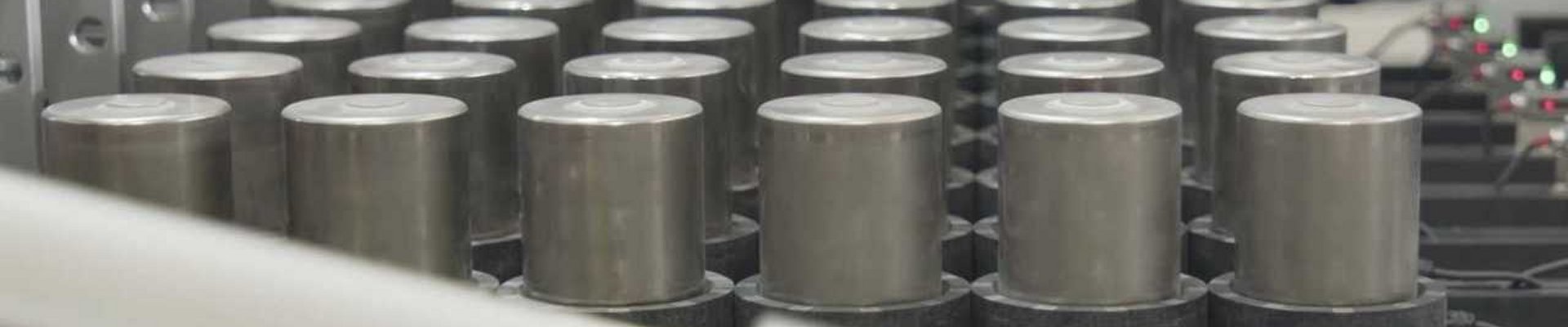
In the Siemens process, trichlorosilane (TCS) gas is decomposed in massive bell-shaped CVD reactors, heated to ~1100°C by electric current through slim silicon rods. This yields ultra-pure polysilicon rods, but with high energy consumption. By contrast, FBR technology feeds silane gas into a fluidized chamber where small silicon seed particles grow into granules. FBR reactors are continuous, less energy-intensive, and increasingly favored for solar-grade polysilicon.
Electrified Process Chain
| Process Step | Electrified Equipment | Role | Electrification Advantage |
|---|---|---|---|
| Chemical Feedstock Preparation | Electrified distillation columns, pumps, compressors | Purification of trichlorosilane or silane gas | High-precision, continuous electric-driven operations |
| Siemens CVD Reactor | Electrically heated rods in bell reactors (~1100°C) | Decomposes TCS into high-purity polysilicon rods | Direct electric heating — inherently an electrified process |
| Fluidized Bed Reactor (FBR) | Electrified fluidization with silane gas feed | Deposits polysilicon granules onto seed particles | Higher energy efficiency, continuous operation, lower capex |
| Post-Processing | Electric crushing, classification, packaging systems | Conditions polysilicon for downstream wafering | Automated electric-mechanical handling with precision sorting |
Role in Industrial Electrification
- Polysilicon production is already electrified — Siemens reactors and FBRs run on direct electricity for heat and fluidization.
- Energy intensity is a critical ESG concern, with pressure to shift supply toward renewable-powered grids or onsite solar + BESS.
- FBR reactors demonstrate how process innovation can cut electricity consumption and carbon footprint.
- The polysilicon industry connects solar PV and semiconductor supply chains, anchoring two of the largest electrification markets.
Market Outlook & Adoption
| Rank | Adoption Segment | Drivers | Constraints |
|---|---|---|---|
| 1 | Solar-Grade Polysilicon | PV demand scaling >1 TW annually; IRA/EU localization efforts | China dominates >75% of supply, high energy footprint |
| 2 | Semiconductor-Grade Polysilicon | Chip industry growth, fab expansions, rad-hard and specialty uses | Ultra-high purity (>11N) requirements, limited producers |
| 3 | FBR Polysilicon | Lower cost and energy intensity, new projects scaling | Still less proven at semiconductor-grade levels |
Strategic Importance
- Core building block for solar PV and semiconductors — electrification of upstream production enables downstream decarbonization.
- Highlights the need for renewable power sourcing in highly energy-intensive industries.
- FBR technology offers a more sustainable, electrification-optimized pathway compared to legacy Siemens reactors.
Downstream Crystal Growth & Wafering
After polysilicon is produced, it is converted into ingots and wafers through fully electrified processes. These steps are distinct but closely linked to polysilicon production, and they showcase additional industrial electrification technologies:
| Process Step | Electrified Equipment | Role | Notes |
|---|---|---|---|
| Crystal Growth (Czochralski, Float Zone) | Induction-heated pullers, crucibles, precision controls | Grows monocrystalline or multicrystalline silicon ingots | Relies on electric induction heating; energy-intensive but electrified by design |
| Ingot Slicing (Wafering) | Electric wire saws, plasma-assisted cutting | Slices ingots into wafers for solar cells and semiconductors | Automation and robotics optimize yield and reduce kerf loss |
| Wafer Cleaning & Polishing | Electric plasma etchers, CMP (chemical-mechanical polishing) tools | Prepares wafers for cell diffusion or chip fabrication | Plasma and CMP tools are electricity-driven, enabling cleanroom automation |
It is important to note here that crystal growth, ingot slicing, and wafer processing are already fully electrified processes. This places them firmly within the broader context of industrial electrification, even as they remain more closely tied to semiconductor and PV supply chains.